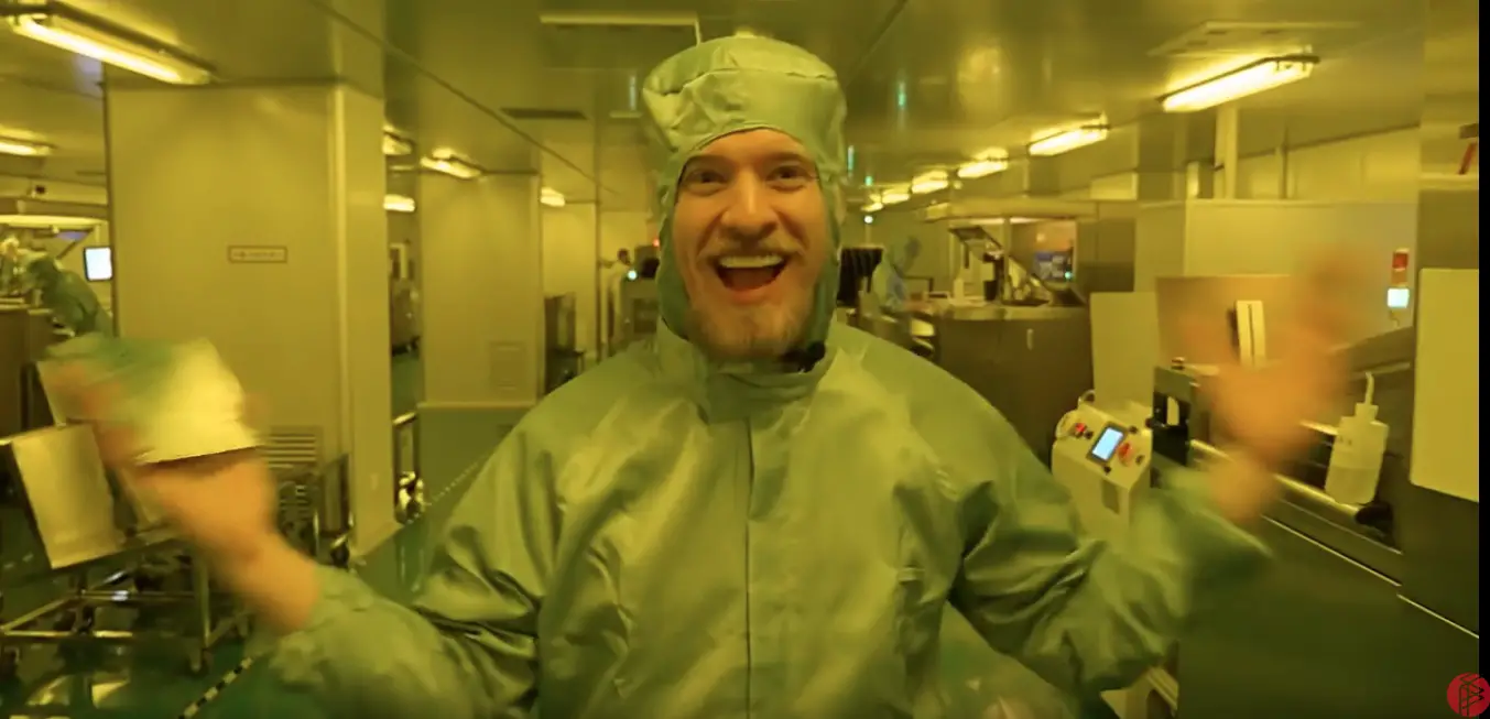
Curious how the printed circuit boards in electronics gadgets are made? Scotty from Strange Parts takes us to a PCB Factory in China, showing us the manufacturing process from design files to the finished product.
The following is part of the process shown in the video. A big take-away is what he did not mention -- there are many steps involving various chemicals, and it's not discussed what happens to those chemicals. When copper is etched off the board, is the copper reused? Are the chemicals toxic? Are the chemicals disposed of properly?
This is in China, a country not known for ecological standards. It's possible the process uses toxic chemicals that are simply dumped into the local river.
Recovery of etched copper could be very important since copper is a rare material. The rareness of copper might be enough incentive for the companies to recover copper from the etching process?
All images are of course copyright to Strange Parts. I did not request permission, but I believe they will like what I've done here.
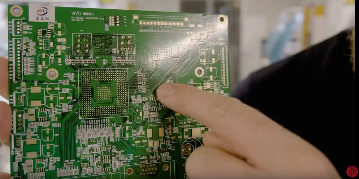
In a typical printed circuit board is copper wiring sandwiched between layers of fiberglass. The result is a 3-Dimensional maze of copper wiring making up the electrical circuit. The idea is to connect the components on the PCB together to form the electrical circuit. Fitting the circuitry into the available space requires using multiple layers of wiring.
Source: Strange Parts
Old-school printed circuit boards like I made in my bedroom in the 1970's were a single layer - copper coated on one side of the board, you draw the circuit using an ink-resist pen, then process the board to etch off the copper, then finally solder components to the board. Modern circuit boards are much more complex than that, of course.
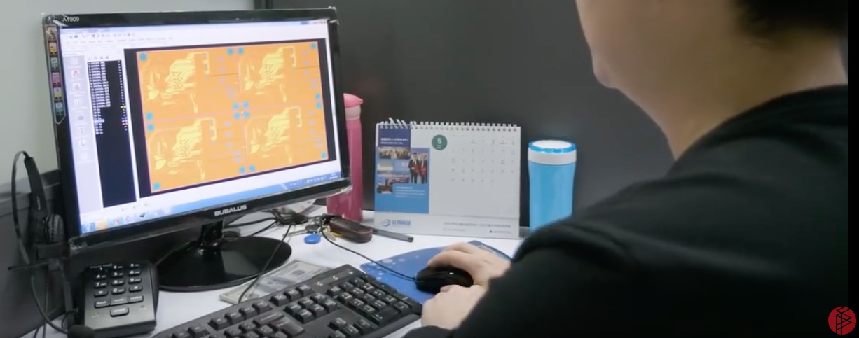
An engineer checking the design file to ensure the PCB is manufacturable. The "layer lists" must work out correctly, etc. This engineer makes the "production file", sending it over the Internet to the factory.
Source: Strange Parts
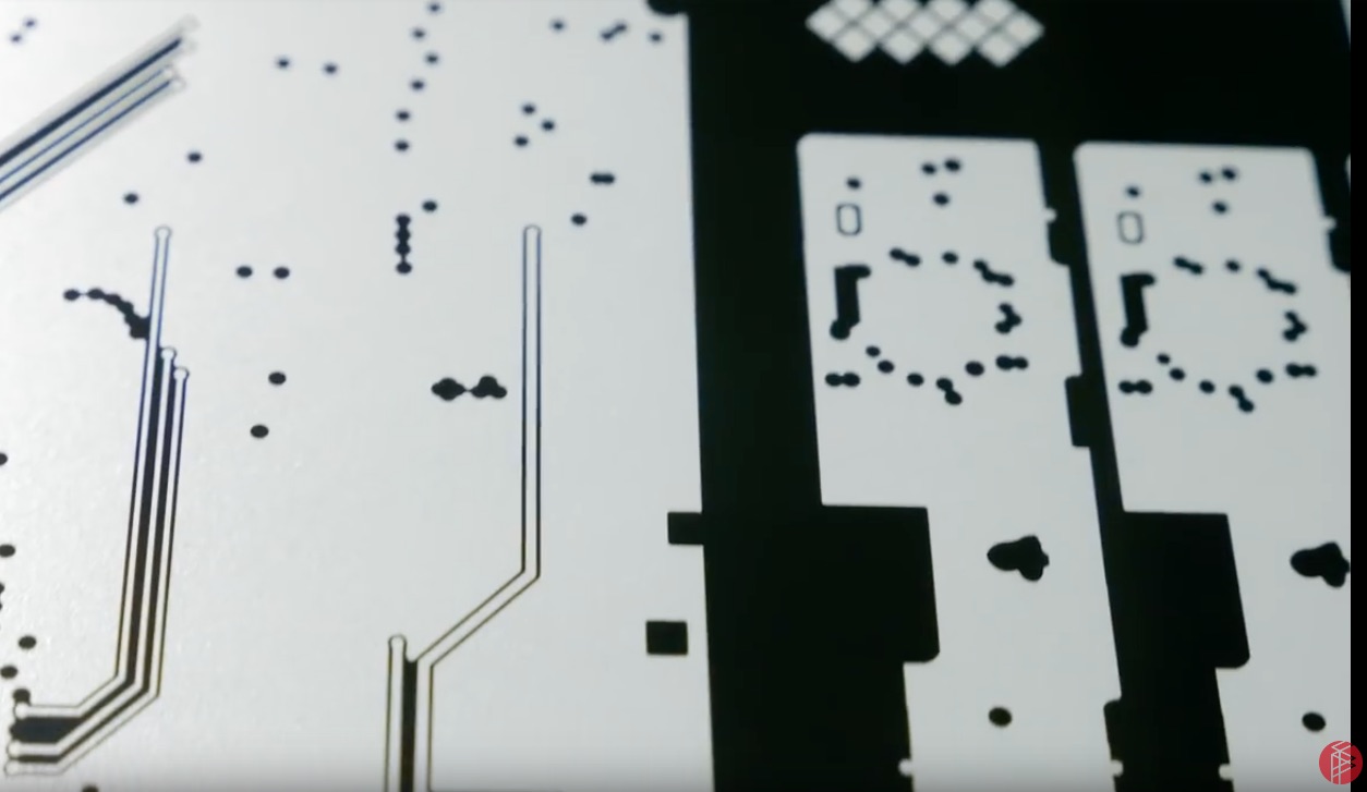
The design for individual layers is printed onto clear film. Light is projected through this film onto a board with photoresist.
Source: Strange Parts
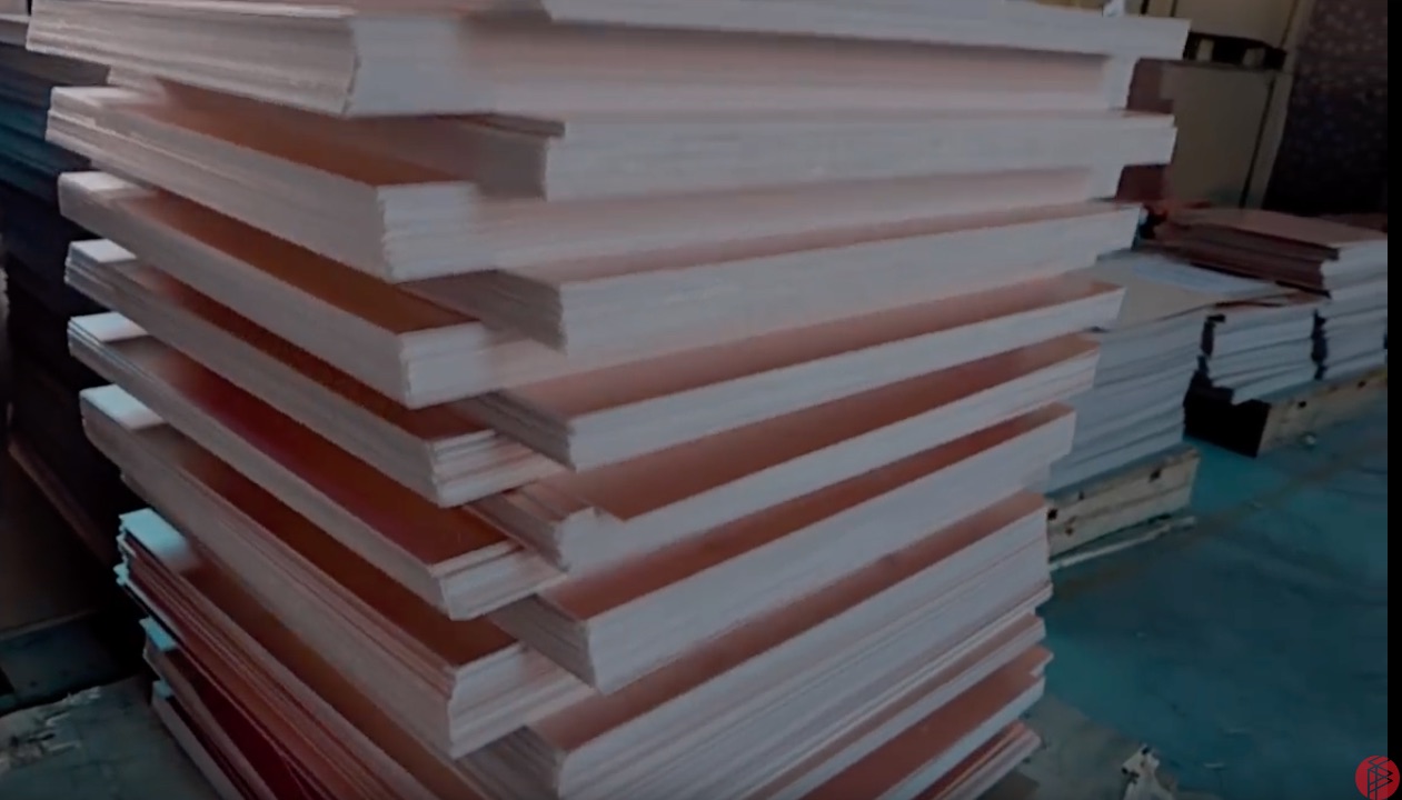
Sheets of FR-4 fiberglass board ready to be made into printed circuit boards. The sheets are large, and of course they are cut to size required by the given board. There is a layer of copper on top and bottom.
Source: Strange Parts
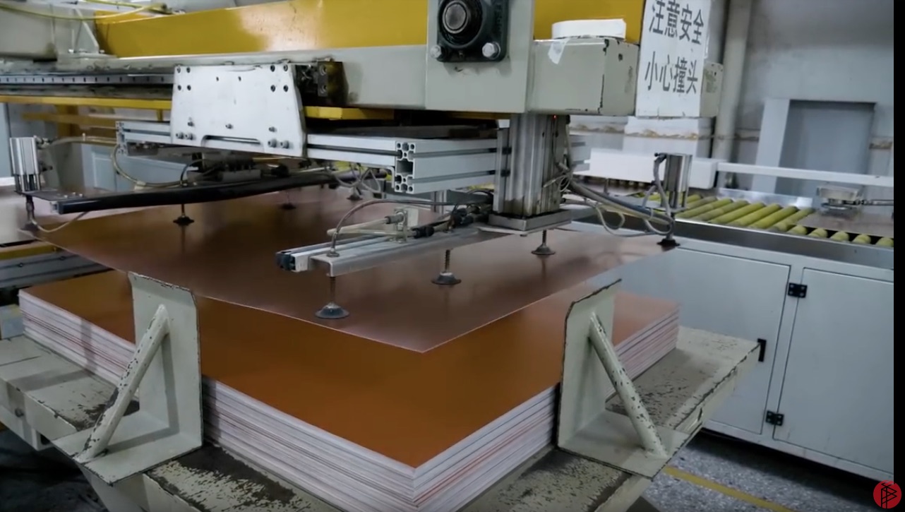
The boards are sent through automated cutting machines that are gigantic saws cutting the sheets into the size required by the board being produced.
Source: Strange Parts
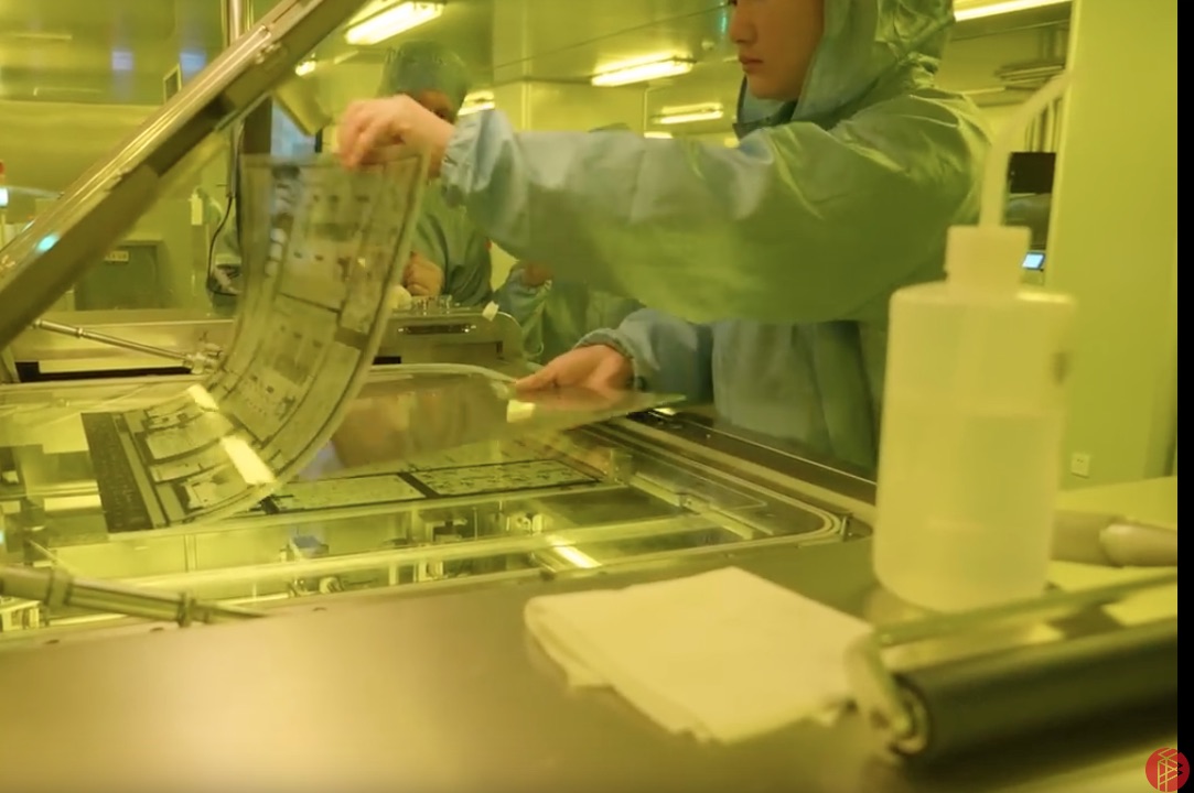
In a special room, a photo-resist chemical is applied to the boards. This chemical "hardens" when exposed to white light, and does not harden in yellow light, hence the overall color of the room. The process requires clean-room conditions, hence everyone wears the bunny suits and passes through an air lock. On a machine similar to a photocopy machine, each sheet is placed between two instances of the film, so that both sides of the sheet is exposed to light. That prints the circuit pattern onto the copper.
Source: Strange Parts
The developing process happens in these machines. Everywhere there is remaining copper, not covered by the photoresist ink, the copper will be removed. In one stage "excess" photo-resist is washed off. Then an alkiline solution removes the copper.
Source: Strange Parts
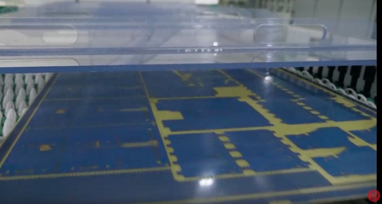
Here is the board with excess copper dissolved away. The yellow is the underlying fiberglass (FR-4) showing through. Afterwards the remaining photo-resist ink is washed away.
Source: Strange Parts
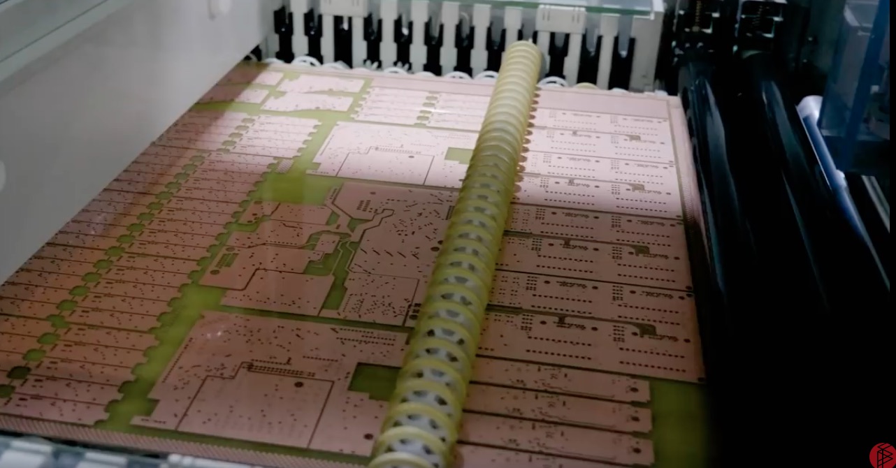
The ink has been washed away, leaving copper and fiberglass.
Source: Strange Parts
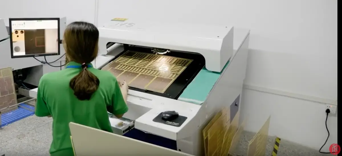
An Automatic robotic inspection of the layers to ensure everything was printed correctly.
Source: Strange Parts
About the Author(s)
David Herron:
David Herron is a writer and software engineer focusing on the wise use of technology. He is especially interested in clean energy technologies like solar power, wind power, and electric cars. David worked for nearly 30 years in Silicon Valley on software ranging from electronic mail systems, to video streaming, to the Java programming language, and has published several books on Node.js programming and electric vehicles.